|
|
||
|---|---|---|
| .. | ||
| rev1 | ||
| rev2 | ||
| README.md | ||
README.md
CaribouLite Hardware Revisions
CaribouLite board has two revisions:
- Rev1: A prototyping revision (the red board).
- Rev2: Production revision.
This documentation shall cover the production revision board (rev2).
System Diagram
 |
| CaribouLite SDR System Diagram |
Power Distribution
To simplify the board and its interfacing to the Raspberry Pi computer, all components on board operate with 3.3V. The FPGA further requires also 1.2V and 2.5V voltages. Two LDO components have been used to derive these voltages from the RPI 5V output voltage.
The usage of LDOs provides high level of voltage isolation, low emitted noise, and design simplicity. The downside of such choise it the dissipated heat from the LDOs. This heat is controlled by providing descent heat sinking to the board through the power planes and adjucent metalic elements (i.g. connectors).
The power distribution provides high frequency isolation of the RF components from the digital components (memory, RPI and FPGA) at frequencies lower than 10 MHz. Above 100 MHz additional isolation is provided by using ferrite beads with high impedance (>500 Ohms) at 100MHz. A set of filterring bypass capacitors have been chosen to further suppress noise generated by components on their power lines at mid-range frequencies (10 to 100 MHz) - the set contains 1nF, 100 nF and 4.7uF capacitors bypassing power and data lines effective at the said frequency ranges.
RPI HAT EEPROM
An I2C EEPROM device is assembled on CaribouLite to support for the requirements of RPI HATs as described in RPI HAT Requirements. For the first setup of the device, the write-protect pin of the EEPROM needs to be released (de-asserted). To do so, the USR-Switch needs to be pushed all along the programming period, and released as the operation completes.
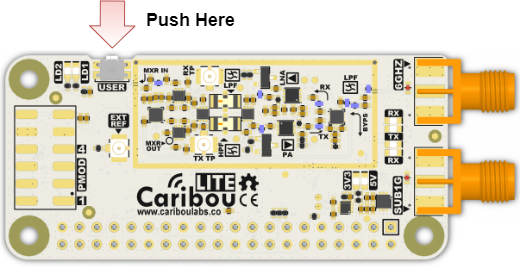 |
| User Switch to push when programming EEPROM |
Clocking
The FPGA is externally clocked by a crystal oscillator of 125MHz located in the bottom side of the board. Clocking the FPGA from the RPI GPCLK (GPIO4 / GPCLK0 / SMI_SA1) is also possible but not recommanded as it may cause substancial increase in the board EMI. For that reason, the GPCLK option is possible but not used in the mainline hardware version. Hacking the possibility to clock from the RPI is a good idea though.
The MODEM (AT86RF215) is clocked from a 26MHz TCXO (bottom layer). This device provides a stable and low phase noise clock reference to the receivers and transmitters within the IC. The MODEM further outputs a buffered version of the input clock (typically 26MHz, but other possibilities exist as well), to the MIXER input. A capacitor divider circuit adapts the LVCMOS output from the MODEM to the input levels of the MIXER.
The MIXER can also be clocked from a separate dedicated TCXO (not assembled), or an external coherent clock source.
 |
| MIXER clocking options, other than the default MODEM provided reference clock |
PMOD Connector
TBD Synchronization GPS Display Peripherals Maximal current
FPGA and LVDS
TBD
SPI
TBD
RF PATH
TBD
LNA & PA
TBD
Image Rejection and Filterring
TBD
Mixer
TBD
Calibrations & Testing
TBD Test points
Hacks
TBD mixerless system
License

This work is licensed under a Creative Commons Attribution 4.0 International License.